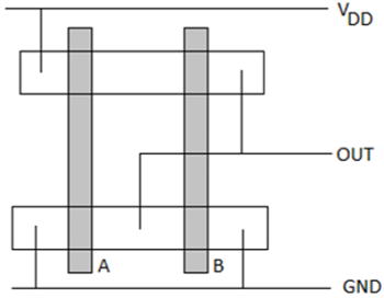
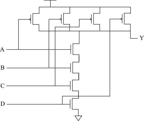
10+ sketch a stick diagram for a cmos 4-input nor gate
See the answer See the answer See the answer done loading. To learn how to draw stick diagrams for a given MOS circuit.

Stick Diagrams Unit Iii Vlsi Circuit Design Processes Vlsi Design Ppt Download
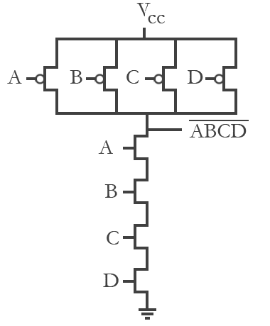
Now lets understand how this circuit will behave like a NOR gate.

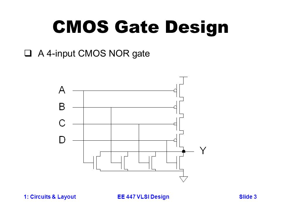
. The above drawn circuit is a 2-input CMOS NOR gate. 1 answer below Estimate the area of your 4-input NOR gate from Exercise 110. EulerPaths CMOS VLSI Design Slide 3 Complex Circuit Layouts Single diffusion runs Multiple Diffusion runs C AB AB EulerPaths CMOS VLSI Design Slide 4 4-Input NAND Gate Sticks.
Exercise 15 Sketch a transistor-level schematic for a CMOS 4-input NOR gate. VA Low VB Low. Assignment 02 1.
Sketch a stick diagram for a CMOS 4-input NOR gate from Exercise. Exercise 110 Sketch a stick diagram for a CMOS 4-input NOR. This problem has been solved.
View Homework Help - Exam 1805pdf from MATH 154 at CUNY Hunter College. And also Sketch a stick diagram for a CMOS 4-input NOR gate from Exercise 15. To know what is meant by stick diagram.
Ii Estimate the area of your 4-input NOR gate from. Exercise 110 Sketch a stick. Exercise 110 Sketch a stick diagram for a CMOS 4-input NOR gate from Exercise 15.
To understand the capabilities and limitations of stick diagram. I Sketch a stick diagram for a CMOS 4-input NOR gate.
![]()
Sketch Of Pulse Widening Effect On Lossy Unterminated Transmission Download Scientific Diagram

M2 Media Studios Where Communications Professionals Master The Media

Stick Diagrams Unit Iii Vlsi Circuit Design Processes Vlsi Design Ppt Download

Exam 1805 Pdf Question Sketch A Stick Diagram For A Cmos 4 Input Nor Gate From Exercise Exercise Sketch A Transistor Level Schematic For A Cmos Course Hero

Exam 1805 Pdf Question Sketch A Stick Diagram For A Cmos 4 Input Nor Gate From Exercise Exercise Sketch A Transistor Level Schematic For A Cmos Course Hero

Sheet 5 Sheet 5 Layout And Stick Diagram 1 For A Cmos 4 Input Nor Gate A Sketch A Transistor Level Schematic B Sketch A Stick Diagram C Estimate Course Hero
Download Block Gsi Helmholtzzentrum Fur Schwerionenforschung

Ion Beam Induced Surface And Interface Engineering Sciencedirect
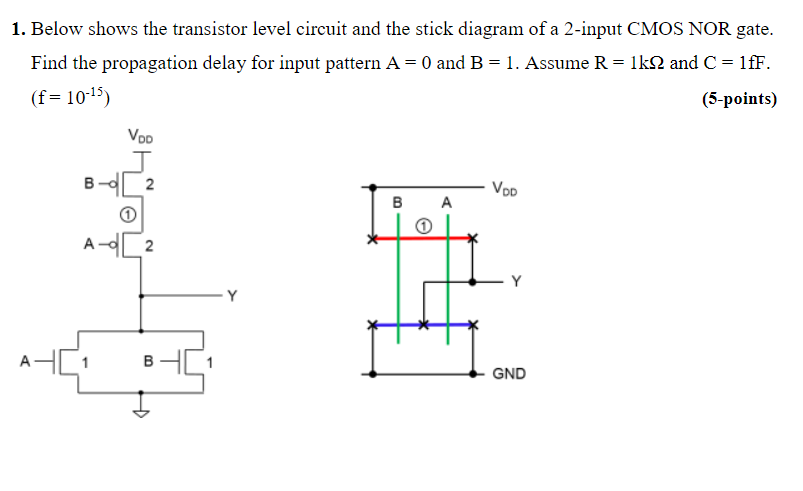
Solved 1 Below Shows The Transistor Level Circuit And The Chegg Com
Combinational Mos Logic Circuits

How To Draw Nor Gate Layout Diagram Youtube
Vlsi Design Circuits Layout Ppt Video Online Download
Solved Chapter 4 Problem 9e Solution Cmos Vlsi Design 4th Edition Chegg Com

Stick Diagrams Unit Iii Vlsi Circuit Design Processes Vlsi Design Ppt Download
E77 Lab 3 Laying Out Simple Circuits

Vlsi Design Dica Chapter 1 Topic 2 Cmos Logic
1 Archive Server